Understand each stage of the production process:
Project: Gauss engineers define the electrical lines and the placement of components in a layout. Thereafter, several photolithographed images are produced which subsequently can be used to the printing of circuit lines and masks.
Laser scribing: Gauss has the only Lumonics V150 equipment in brazilian Market, used for substrate scribing. The cutting lines made in the substrate by this laser gun separate circuits.
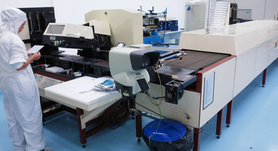
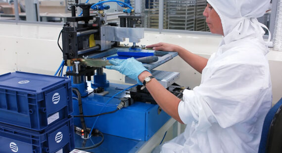
Printing of conductors: Using the system of high precision screen printing, with automated devices and cameras for the perfect adjustment of the screens, which allows the creation of conductors in the circuit.
Firing: After drying the printed conductors, the substrate goes through a furnace at 850ºC. The high temperature allows the printing material to turn into low resistivity metal.
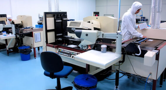
Printing of resistors: At this stage, the resistors are screend printed. Then the pieces are subjected to a new resistive mass acquires the consistency needed and electrical properties are defined.
Resistors trimming: using laser trimming on active or passive way to ensure that each resistor will get the exact value of the project designed. This technology ensures tolerances of 5% to 0.25%.
Coverage printing: a layer of coverage (organic/glass) is applied to protect the resistors and the conducting lines against oxidation. This step is where Gauss enhances the stability of the circuit and the quality of the process.
SMD Assembly: Here, Gauss assembles the electronics by Surface Mounting Device technology.
Inspections and final tests: to conclude the process, optical and visual inspections are performed, circuit to circuit, as well as individual dynamic tests. Everything to guarantee the full functionality of the product delivered to our customers.
Materials used:
a) Ceramic substrate
– Material: Ceramic aluminum oxide (96% AL2O3)
– Dimensions: 6.5 x 5.4 inches
– Thickness: 0.635 mm std, 1.2 mm max
– Density: 3.7 g / cm3
– Thermal conductivity: 0.35 W / cm * K @ 25C
– Electrical resistance: 10 ^ 14 Ohm * cm
– Dielectric constant: 9.5
b) Conductive Binders
– Material: PdAg 30mOhm / sq, PtAg 4 mOhm / sq, Ag 2 mOhm / sq, Au 3 mOhm / sq
– Minimum Width: 0.10 mm
– Minimum spacing: 0.10 mm
c) Resistive Folders:
– Resistivity: 10 mOhm / sq to 100 MOhm / sq
– Resistance Range: 0.1 Ohm to 1 GOhm
– Tolerance: 5% to 0.25% (ratio 0.15%)
– tc: 100 ppm / K to 15 ppm / K T = -55 C to 125 C
– Power: 300 mW / mm2
d) Capacitive folders
– Capacitance: 2 pF / mm2 to 200 pF / mm2
– Tolerance: +/- 20%
e) Inductive binders
Inductance: 2 nH to 100 nH
– Tolerance: + – 20%